- 您现在的位置:买卖IC网 > Sheet目录2002 > KAD5512HP-17Q72 (Intersil)IC ADC 12BIT 170MSPS SGL 72-QFN
19
FN6808.3
October 1, 2009
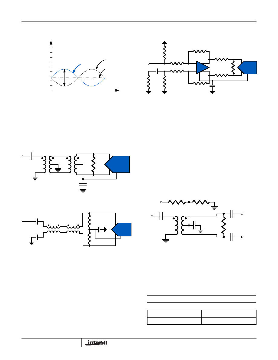
full-scale input voltage is 1.45V, centered at the VCM voltage
of 0.535V as shown in Figure 25.
Best performance is obtained when the analog inputs are
driven differentially. The common-mode output voltage,
VCM, should be used to properly bias the inputs as shown in
noise and distortion performance for wideband and/or high
intermediate frequency (IF) inputs. Two different transformer
This dual transformer scheme is used to improve common-
mode rejection, which keeps the common-mode level of the
input matched to VCM. The value of the shunt resistor
should be determined based on the desired load impedance.
The differential input resistance of the KAD5512HP is 500
Ω.
The SHA design uses a switched capacitor input stage (see
Figure 41), which creates current spikes when the sampling
capacitance is reconnected to the input voltage. This causes
a disturbance at the input which must settle before the next
sampling point. Lower source impedance will result in faster
settling and improved performance. Therefore a 1:1
transformer and low shunt resistance are recommended for
optimal performance.
A differential amplifier, as shown in Figure 28, can be used in
applications that require DC-coupling. In this configuration
the amplifier will typically dominate the achievable SNR and
distortion performance.
Clock Input
The clock input circuit is a differential pair (see Figure 42).
Driving these inputs with a high level (up to 1.8VP-P on each
input) sine or square wave will provide the lowest jitter
performance. A transformer with 4:1 impedance ratio will
provide increased drive levels.
The recommended drive circuit is shown in Figure 29. A duty
range of 40% to 60% is acceptable. The clock can be driven
single-ended, but this will reduce the edge rate and may
impact SNR performance. The clock inputs are internally
self-biased to AVDD/2 to facilitate AC-coupling.
A selectable 2x frequency divider is provided in series with
the clock input. The divider can be used in the 2x mode with
a sample clock equal to twice the desired sample rate. This
allows the use of the Phase Slip feature, which enables
synchronization of multiple ADCs.
FIGURE 25. ANALOG INPUT RANGE
1.0
1.8
0.6
0.2
1.4
INP
INN
VCM
0.535V
0.725V
FIGURE 26. TRANSFORMER INPUT FOR GENERAL
PURPOSE APPLICATIONS
ADT1-1WT
0.1F
KAD5512HP
VCM
ADT1-1WT
1000pF
FIGURE 27. TRANSMISSION-LINE TRANSFORMER INPUT
FOR HIGH IF APPLICATIONS
ADTL1-12
0.1F
KAD5512HP
VCM
ADTL1-12
1000pF
TABLE 1. CLKDIV PIN SETTINGS
CLKDIV PIN
DIVIDE RATIO
AVSS
2
Float
1
AVDD
4
FIGURE 28. DIFFERENTIAL AMPLIFIER INPUT
KAD5512HP
VCM
0.1F
0.22F
69.8O
49.9O
100O
69.8O
348O
CM
217O
25O
Ω
FIGURE 29. RECOMMENDED CLOCK DRIVE
TC4-1W
200pF
AVDD
200O
200pF
CLKP
CLKN
1kO
1000pF
Ω
KAD5512HP
发布紧急采购,3分钟左右您将得到回复。
相关PDF资料
KAD5512P-17Q72
IC ADC 12BIT 170MSPS SGL 72-QFN
KAD5514P-12Q72
IC ADC 14BIT 125MSPS SGL 72-QFN
KAD5610P-25Q72
IC ADC 10BIT 250MSPS DUAL 72-QFN
KAD5612P-17Q72
IC ADC 12BIT 170MSPS DUAL 72-QFN
LA72715NV-TLM-E
IC AUDIO DECODER JPN MTS 24SSOP
LICAL-DEC-LS001
IC DECODER LOW SECURITY 8DIP
LICAL-DEC-MS001
IC DECODER MS SERIES 20-SSOP
LICAL-ENC-MS001
IC ENCODER MS SERIES 20-SSOP
相关代理商/技术参数
KAD5512HP-21Q48
功能描述:模数转换器 - ADC 12-BIT 210MSPS HI PERF SINGLE ADC PROG
RoHS:否 制造商:Texas Instruments 通道数量:2 结构:Sigma-Delta 转换速率:125 SPs to 8 KSPs 分辨率:24 bit 输入类型:Differential 信噪比:107 dB 接口类型:SPI 工作电源电压:1.7 V to 3.6 V, 2.7 V to 5.25 V 最大工作温度:+ 85 C 安装风格:SMD/SMT 封装 / 箱体:VQFN-32
KAD5512HP-21Q72
功能描述:模数转换器 - ADC 12-BIT 210MSPS HI PERF SINGLE ADC PROG
RoHS:否 制造商:Texas Instruments 通道数量:2 结构:Sigma-Delta 转换速率:125 SPs to 8 KSPs 分辨率:24 bit 输入类型:Differential 信噪比:107 dB 接口类型:SPI 工作电源电压:1.7 V to 3.6 V, 2.7 V to 5.25 V 最大工作温度:+ 85 C 安装风格:SMD/SMT 封装 / 箱体:VQFN-32
KAD5512HP-25Q48
功能描述:模数转换器 - ADC 12-BIT 250MSPS HI PERF SINGLE ADC
RoHS:否 制造商:Texas Instruments 通道数量:2 结构:Sigma-Delta 转换速率:125 SPs to 8 KSPs 分辨率:24 bit 输入类型:Differential 信噪比:107 dB 接口类型:SPI 工作电源电压:1.7 V to 3.6 V, 2.7 V to 5.25 V 最大工作温度:+ 85 C 安装风格:SMD/SMT 封装 / 箱体:VQFN-32
KAD5512HP-25Q72
功能描述:模数转换器 - ADC 12-BIT 250MSPS HI PERF SINGLE ADC
RoHS:否 制造商:Texas Instruments 通道数量:2 结构:Sigma-Delta 转换速率:125 SPs to 8 KSPs 分辨率:24 bit 输入类型:Differential 信噪比:107 dB 接口类型:SPI 工作电源电压:1.7 V to 3.6 V, 2.7 V to 5.25 V 最大工作温度:+ 85 C 安装风格:SMD/SMT 封装 / 箱体:VQFN-32
KAD5512P
制造商:INTERSIL 制造商全称:Intersil Corporation 功能描述:Low Power 12-Bit, 250/210/170/125MSPS ADC
KAD5512P_09
制造商:INTERSIL 制造商全称:Intersil Corporation 功能描述:Low Power 12-Bit, 250/210/170/125MSPS ADC
KAD5512P-12Q48
功能描述:模数转换器 - ADC 12-BIT 125MSPS SINGL ADC PROG LVDS/LVCMOS RoHS:否 制造商:Texas Instruments 通道数量:2 结构:Sigma-Delta 转换速率:125 SPs to 8 KSPs 分辨率:24 bit 输入类型:Differential 信噪比:107 dB 接口类型:SPI 工作电源电压:1.7 V to 3.6 V, 2.7 V to 5.25 V 最大工作温度:+ 85 C 安装风格:SMD/SMT 封装 / 箱体:VQFN-32
KAD5512P-12Q72
功能描述:模数转换器 - ADC 12-BIT 125MSPS SINGL ADC PROG LVDS/LVCMOS RoHS:否 制造商:Texas Instruments 通道数量:2 结构:Sigma-Delta 转换速率:125 SPs to 8 KSPs 分辨率:24 bit 输入类型:Differential 信噪比:107 dB 接口类型:SPI 工作电源电压:1.7 V to 3.6 V, 2.7 V to 5.25 V 最大工作温度:+ 85 C 安装风格:SMD/SMT 封装 / 箱体:VQFN-32